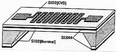
 Fig. 1
MICROMACHINED CIRCUITS for MICROWAVE and MILLIMETER WAVE APPLICATIONS
Romolo Marcelli, Paolo De Gasperis and Claudio Risi
Microwave Microsystem Technology, National Research Council of Italy, Project Sensors and Microsystems (PSM), Research Area of Roma-Tor Vergata, Via del Fosso del Cavaliere 100, 00133 Roma, ITALY
Tel.: +39 06 4993.4536 - Fax: +39 06 4993.4066 - Email: r.marcelli@psm.rm.cnr.it
Alexandru Müller, Ioana Petrini, Viorel Avramescu, Sergiu Iordanescu, Dan Dascalu
National Institute for Research and Development in Microtechnology (IMT), Str. Erou Iancu Nicolae 32B, R72225, Bucuresti, ROMANIA
Giancarlo Bartolucci
University of Roma "Tor Vergata", via di Tor Vergata, 00133 Roma, ITALY
Abstract__It is the aim of this paper to present the first results obtained by our groups regarding the manufacturing of microwave and millimeter wave micromachined devices. Interdigitated capacitors, meander- and S-line inductors as well as a band-stop filter supported by micromachined thin dielectric membranes have been realized. Looking at the obtained results, the micromachining technology offers new perspectives in improving the performances of microwave and millimeter wave devices.
1.INTRODUCTION
In the last decade many studies have been focused on the micromachining of silicon and III-Vs compound semiconductors for high performance sensors. The manufacturing of high quality membranes and cantilevers has stimulated the realization of novel micromachined structures for microelectromechanical systems (MEMS).
Microwave circuit elements manufactured on thin dielectric or semiconducting membranes are one of the most interesting and new applications of MEMS. This new technology was developed by a group of the Ann Arbor University, Michigan [1-3]. In particular, they have demonstrated the feasibility of the "microshield" structure, a transmission line for circuit and antenna applications.
Recently, the realization of micromachined lumped microwave circuit elements - band stop and band pass filters as well as interdigitated capacitors, meander and S-line inductors - was also demonstrated by european groups [4-7].
The major advantages of membrane supported microwave and millimeter wave circuits are the decrease of the dispersion as well as of the dielectric and radiative losses. These results are due to the reduction of the equivalent dielectric permittivity of the substrate to values very close to 1. Owing to the same reason, the resonance frequency of the microwave MEMS is shifted by a factor two with respect to the bulk configurations.
It is the purpose of this paper to present the technological processes for the realization of some microwave and millimeter wave passive circuit elements on micromachined dielectric substrates.
2. MEMBRANE TECHNOLOGY.
The dielectric membrane structure supporting a microwave inductor is presented in Fig.1. High resistivity n-type <100> silicon wafers were first thermally oxidized. Then, a 8000 Å thick silicon dioxide layer was grown, followed by a 2700 Å silicon nitride layer deposited by CVD on both sides of the wafers. Finally, a 4500 Å silicon dioxide layer was grown only on the top of the wafers, also by CVD. This three layer structure avoids any deformation of the membrane, thus compensating the internal stress.
For the realization of lumped elements, a 1.5 µm thin layer (Cr-Au) is evaporated after the deposition of the dielectric layers. To obtain the micromachined structure, the metal layer is patterned and, simultaneously, by a double alignment procedure, windows for membrane etching were opened on the bottom of the wafer. The desired membrane area is determinated, in the case of the anisotropic etching process, by means of the etching angle (54.7º) and by the wafer thickness.
The flatness of the realized membranes is very good, and the standard deviation is less then 0.12 µm for a chip area of about 0.5 mm2.
An atomic force microscope (AFM) was used for the roughness analysis of the membrane supporting the S-line inductors. The maximum measured roughness was 453.5 Å and the average roughness was 18.1 Å. These results confirm the high quality of the membrane.
3. CIRCUIT CONFIGURATIONS AND MICROWAVE MEASUREMENTS.
The first micromachined microwave circuit to be realized was a coplanar band stop filter designed for 16 GHz working frequency. A SEM photo of this circuit supported by the dielectric SiO2 / Si3N4 / SiO2 membrane is presented in Fig.2 and the band-stop response (S21 and S11 scattering parameters) in Fig.3. The propagation losses are sensitively decreased and the resonance frequencies are almost doubled with respect to the bulk configurations, because of the strong decrease of the value of the equivalent permitivity for the micromachined structure.
Two types of interdigitated capacitors, with 8 and 16 fingers respectively, were manufactured with the line and interspace width of 25 µm and a length of 375 µm, on the SiO2 / Si3N4 / SiO2 membrane. In Fig.4 it is shown a SEM photo of the bottom view of a micromachined interdigitated capacitor. One can see the membrane flatness as well as its transparency.
The S parameters measurements for the capacitors have confirmed a value of the resonance frequency which exceeds 50 GHz, this value being the limit of the measuring equipment we have used. The value of this parameter is estimated, from the computed data, over 100 GHz.
Meander and S-line inductors were both realized on the dielectric membranes. The meander-line inductor had a total length of 7 mm (7 meanders) with a line and interspace width of 25 µm, and a line length of 300 µm. In Figs.5-7 SEM photos of the top view, the bottom view and the tilted view of the S-line inductor supported on the 1.5µm thin SiO2 / Si3N4 / SiO2 membrane are shown respectively. One can see the transparency of the membrane as well as the shape of the side walls due to the anisotropic etching process.
The structures were characterized up to 40 GHz using a HP 8510C Network Analyzer with Cascade Microtech probes. Microwave measurements which were in good agreement with computed values of the equivalent circuit parameters have confirmed the significant decrease of the parasitic capacitances induced by the dielectric membrane support.
REFERENCES
Figure Captions.
Fig. 1
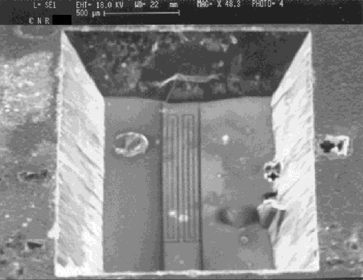 Fig.2
Fig.2
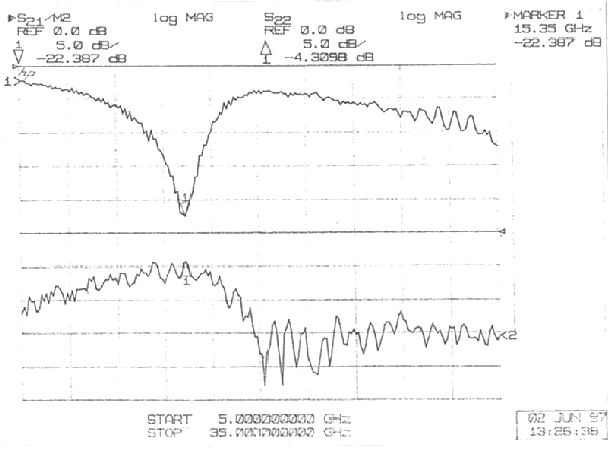 Fig.3
Fig.3
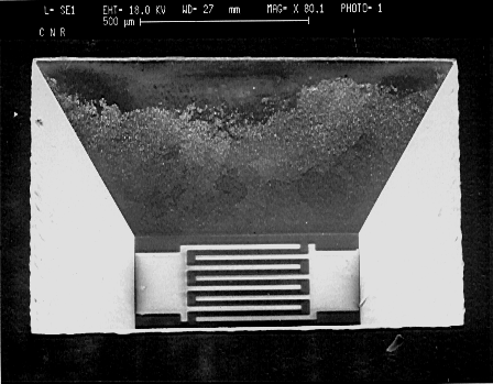 Fig.4
Fig.4
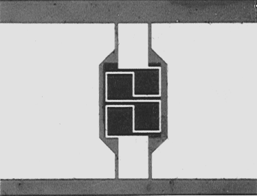 Fig.5.
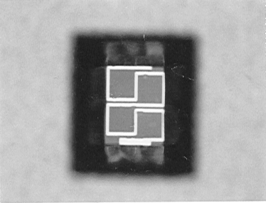 Fig.6.
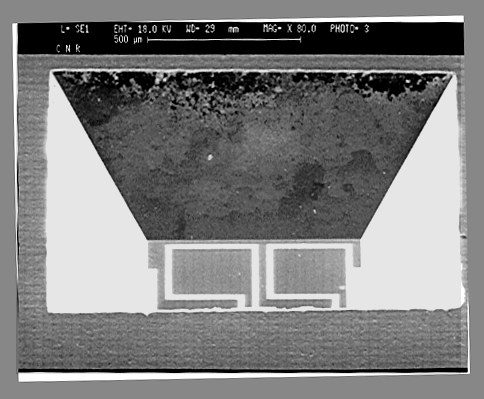 Fig.7.