Annex 2
Micromachined Waveguides for Millimeter Wave Applications
In cooperation with IMT, Bucharest
1. Introduction
Higher and higher frequencies are required by the Communication Systems for Ground and Space Applications currently under development.
The excitation, detection and processing of Millimeter Wave Frequencies is made possible by means of small size device configurations, due to the short wavelengths involved in the propagation. For this reason, Monolithic Microwave Integrated Circuits (MMIC) go towards configurations in which continuous improvements in the miniaturization are needed to accomplish the excitation of millimeter wavelengths. In particular, applications devoted to some specific areas as the automotive one (Collision Avoidance Radar = CAR), the Earth Observation (Radiometry) and the Personal Communications (Wireless Office) need Millimeter Wave Filtering at frequencies higher than 30 GHz (i.e.: f=77 GHz for the Collision Avoidance Radar, f>100 GHz for some Space Applications). In this framework, MMIC or quasi-MMIC device configurations have to be realized caring for reliability and integration with complicated systems.
Recently, micromachined millimeter wave components have been proposed as stubs or waveguide filters, and efforts in realizing different structures have been also presented in. A further refinement of this technique for non-dispersive and low loss micro-waveguides is also discussed in literature.
Simple waveguides as well as more complicated filters can be easily designed by scaling conventional waveguide structures down to the millimeter wave range dimensions. The micromachining process can be performed on Si and GaAs wafers by means of chemical etching and laser techniques. Si is preferred for low cost purposes, but GaAs should be used when high temperature environments are considered.
2. Si and GaAs Micromachining for Microwave Applications (Microwave Microelectromechanical Systems = m W-MEMS).
Non-Si materials like GaAs have been proposed and studied for the realization of microelectromechanical systems (MEMS) to fulfil specific requirements on integration (in subsystems where GaAs MMIC are already present) or on hostile environments (high temperature conditions). On the other hand, Microwave MEMS are appealing technological solutions to be developed on both, Si and GaAs substrates. The goal is the realization of inegrated micro-waveguide components for low power microwave signal processing.
In the last decade many studies have been focused on silicon and III-Vs compound semiconductors micromachining for high performance sensors. The major efforts in the manufacturing of high quality membranes and cantilevers have stimulated the realization of novel micromachined structures.
Manufacturing of microwave circuit elements on thin dielectric or semiconducting membranes is one of the most interesting and new applications of MEMS. This new technology was first developed by a group of Ann Arbor University, Michigan [1-3]. They have reported the "microshield " structure representing a transmission line obtained by means of this new technology for circuit and antenna applications.
Recently, manufacturing of micromachined lumped microwave circuit elements - band stop and pass band filter as well as interdigitated capacitors, meander and S-line inductors - was also reported by european groups [4-7].
The major advantage of membrane supported microwave and millimeter wave circuits consists in the decreasing of the dispersive and radiative losses as a result of the reduction of the substrate equivalent dielectric permittivity to values very close to 1. Owing to the same reason, the resonance frequency of the microwave MEMS is shifted by a factor two with respect to the bulk configurations
It is the purpose of this paper to present the technological processes for manufacturing micromachined microwave structures and the results obtained by our groups about the realization of some microwave and millimeter wave passive circuit elements on micromachined dielectric substrates.
3. Dielectric membrane manufacturing using anisotropic etching of high resistivity <100> silicon
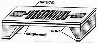
The manufactured dielectric membrane structure suporting a microwave inductor is presented in Fig.1. High resistivity n-type <100> silicon wafers were first thermally oxidised. Then a 8000Å thick silicon dioxide layer was grown, followed by a 2700Å silicon nitride layer deposited by CVD on both sides of the wafers. Finally, a 4500Å silicon dioxide layer was grown only on the top of the wafers, also by CVD.
Fig.1. Schematic view of the three layer membrane supporting a microwave circuit.
This three layer structure avoids any deformation of the membrane, thus compensating the internal stress. Moreover, the propagation losses are considerablly improved and the resonance frequencies are almost doubled with respect to the bulk configurations, being the value of the equivalent permitivity e » 1 for the structure shown in Fig.1.
&#For lumped elements manufacturing, a 1.5 µm thin layer (Cr-Au) is evaporated after the dielectric layers deposition.. In order to obtain the micromachined structure, the metal layer is patterned and, simultaneously, by a double alignment procedure, windows for membrane etching were opened on the bottom of the wafer. The desired membrane area is determinated, in the case of anisotropic etching process, by means of the etching angle (54.7º) and by the wafer thickness.
The flatness of the realised membranes is very good, and the standard deviation is less then 0.12µm for a chip area of about 0.5mm2.
An atomic force microscope (AFM) was used for the roughness analysis of the membrane supporting the S-line inductors. The maximum measured roughness was 453.5 Å and the average roughness was 18.1 Å. These results confirm the high quality of the
manufactured membrane.
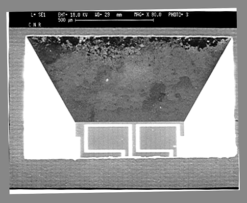
The first micromachined microwave circuit to be manufactured was a coplanar band stop filter designed for 16GHz working frequency. A SEM photo of this circuit supported by the dielectric SiO2 / Si3N4 / SiO2 membrane is presented in Fig.2 and the band-stop response (S21 and S11 parameters) in Fig.3.
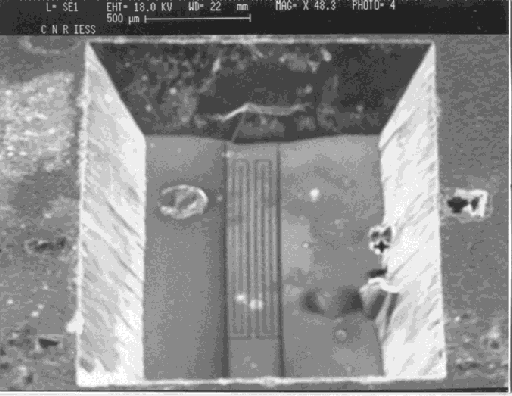
Fig.2. SEM photo of a micromachined band-stop filter.
Two types of interdigitated capacitors, with 8 and 16 fingers respectively, were manufactured with the line and interspace width of 25µm and a length of 375µm, on the SiO2 / Si3N4 / SiO2 membrane. In Fig.4 it is shown a SEM photo of the bottom view of a micromachined interdigitated capacitor. One can see the membrane flatness as well as its transparency.
The S parameters measurements for the capacitors have confirmed a value of the resonance frequency which exceeds 50 GHz, this value being the limit of the measuring equipment we have used. The value of this parameter is estimated, from the computed data, over 100GHz. Similar capacitors manufactured on S.I. GaAs have exhibited a resonance frequency of 40GHz.
Meander and S-line inductors were manufactured on the dielectric membranes; the meander-line inductor has a total length of 7mm (7 meanders) with a line and interspace width of 25µm, and a line length of 300 µm. In Figs.5-7 there are presented a top view, a bottom view and a SEM photo of the S-line inductor supported on the 1.5µm thin SiO2 / Si3N4 / SiO2 membrane. One can see the transparency of the membrane as well as the shape of the side walls due to the anisotropic etching process.
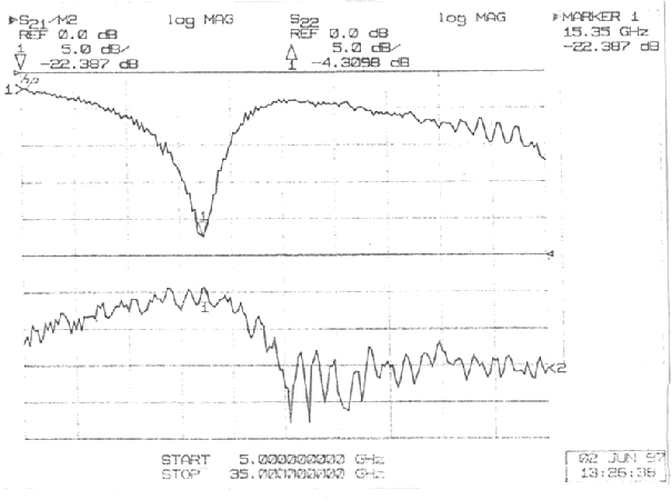
Fig.3. Band-stop response of the filter of Fig.2.
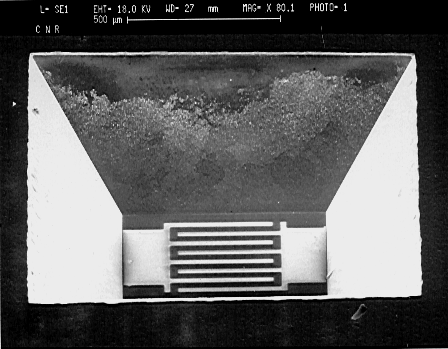
Fig.4. SEM photo of a micromachined interdigitated capacitor
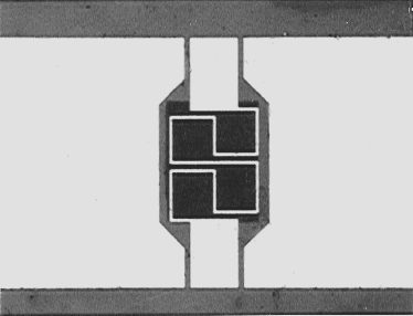
Fig.5 Top view of an S-line micromachined inductor
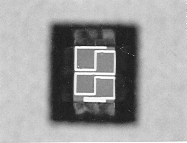
Fig.6. Bottom view of an S-line micromachined inductor
Side walls of the S-line inductor substrate
The structures were characterized up to 40GHz using a HP 8510C Network Analyzer with Cascade Microtech probes. Microwave measurements which were in good agreement with computed values of the equivalent circuit parameters have confirmed the significant decreasing of the parasitic capacitances induced by the dielectric membrane support.
REFERENCES
Further General References on Micromachined Microwave Devices
[1] T.M. Weller and L. P.B. Katehi: "Compact Stubs for Micromachined Coplanar Waveguide", Proceed. of the 25th European Microwave Conference, Bologna, Italy, 589 (1995).
[2] S. Lucyszyn et al: "Design of Low-loss Monolithic Millimeter-wave Filters Using Dielectric-filled Metal-pipe Rectangular Waveguides"; Proceed. of the ESA/ESTEC Workshop on CAD for Microwave Filters, Norrwijk, The Netherlands (1995).
[3] R.F. Drayton and L.P.B. Katehi: "Development of Miniature Microwave Circuit Components Using Micromachining Techniques", Proceed. of 1994 Microwave Theory and Techniques Symposium (MTT-S), 225 (1994).
[4] S. Robertson, L.P.B. Katehi, and G.M. Rebeiz: "Micromachined W Band Filters", IEEE Trans. on Microwave Theory and Tech., Vol.44, No.4, 598 (1996).